|
|
|
Introduction:
SMT PCB Assembly means Surface Mount Technology, known as a a kind of Circuit assembly technology that installs the SMC/SMD (named Chip Components in Chinese) on the surface of Printed Circuit Board or on the surface of other substrates, which is solded and assembled by means of reflow soldering or dip soldering. It realizes high density, high reliability, miniaturization and low cost of electronic product assembly.
Characterictics:
1. High density, small size, low weight;
2. Reliable, strong earthquake resistance and low defect rate of soldering spot;
3. High frequency, reducting the interference of electromagnetism and radio frequency;
4. Easy to realize automation and improve production efficiency.
Product Details:
Payment & Shipping Terms:
|
| Layer Count: | 2 ` 30 Layers | Max Board Size: | 600 Mm X 1200 Mm |
|---|---|---|---|
| Base Material For PCB: | FR4, CEM-1, TACONIC, Aluminium, High Tg Material, High Frequence ROGERS ,TEFLON, ARLON, Halogen-free Material | Rang Of Finish Baords Thickness: | 0.21-7.0mm |
| Minimum Line Width: | 3mil (0.075mm) | Minimum Line Space: | 3mil (0.075mm) |
| Minimum Hole Diameter: | 0.10 Mm | E-Testing: | 100% E-Testing (High Voltage Testing); Flying Probe Testing |
| High Light: | 30L FR4 SMT PCB Assembly,SMT PCB Assembly 7.0mm Thickness,Lead Free HASL Pcb Prototype Board |
||
Ultrafast PCB fabrication manufacturer, offering one-stop PCB manufacturing, PCB assembly, SMT stencil,cheap and good quality pcb smt assembly
1. Features
1. One Stop OEM Service, PCB manufacturing Made in Shenzhen of China
2. Manufactured by Gerber File and BOM List from Customer
3. FR4 Material, Meet 94V0 standard
4. SMT, DIP technology suport
5. Lead Free HASL, Environmental Protection
6. UL, CE, ROHS Compliant
7. Shipping By DHL,UPS, TNT, EMS or Customer requirement
2. PCB Technical capability
| SMT | Position accuracy:20 um |
| Components size:0.4×0.2mm(01005) —130×79mm,Flip-CHIP,QFP,BGA,POP | |
| Max. component height::25mm | |
| Max. PCB size:680×500mm | |
| Min. PCB size:no limited | |
| PCB thickness:0.3 to 6mm | |
| PCB weight:3KG | |
| Wave-Solder | Max. PCB width:450mm |
| Min. PCB width: no limited | |
| Component height:Top 120mm/Bot 15mm | |
| Sweat-Solder | Metal type :part, whole, inlay, sidestep |
| Metal material:Copper , Aluminum | |
| Surface Finish:plating Au, plating sliver , plating Sn | |
| Air bladder rate:less than20% | |
| Press-fit | Press range:0-50KN |
| Max. PCB size:800X600mm | |
| Testing | ICT,Probe flying,burn-in,function test,temperature cycling |
3.PCB Manufacturing Process
4.The PCB Fabrication Process
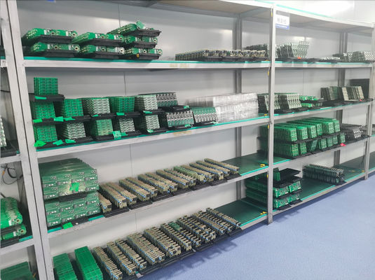
5.PCB Pictures
![]()
![]()
Contact Person: Mrs. Helen Jiang
Tel: 86-18118756023
Fax: 86-755-85258059