|
What is a multilayer PCB?
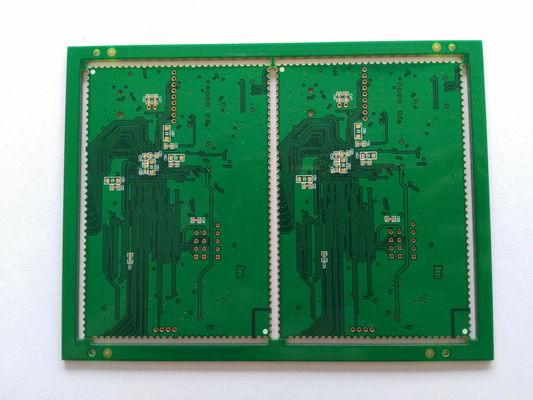
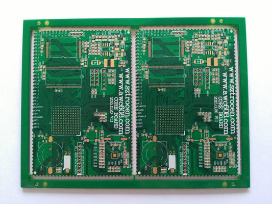
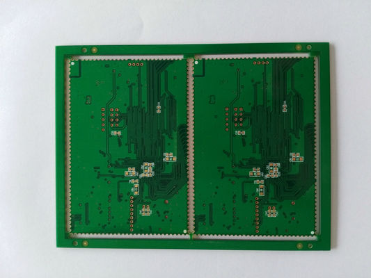
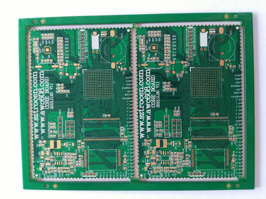
In simple terms, a multilayer board is a printed circuit board with more than two layers and at least three layers of conductive material or copper. When looking at a multilayer PCB, the top and bottom layers look similar to a double-sided PCB, but they have more layers on both sides of the core. The layers are interconnected through copper plated vias and there can be more layers, we have witnessed up to 40 layers. Active and passive components are placed on the top and bottom layers of a multilayer PCB, while the internal stacked layers are used for routing.
As multilayer PCBs can accommodate more electronic components, they are widely used in modern electrical appliances, with the number of layers ranging from four to twelve. Several applications such as smart devices require four to eight layers, while smartphones can use up to twelve layers. When manufacturing a multilayer PCB, designers will choose an even number of layers instead of an odd number of layers, because laminating an odd number of layers makes the circuit complex and the cost will also be high.
Why we need it:
Cause the increased concentration of integrated circuit package leading to a high concentration of interconnect lines, It makes it necessory to use the multiple substrates.
Unpredictable design issues such as noise, stray capacitance, crosstalk, etc. occur in the layout of the PCB. Therefore, the design of PCB must focus on minimizing the length of the signal line and avoiding parallel paths.
Obviously, due to the limited number of crossovers that can be achieved in a single-side, even in a double-side board, these requirements cannot be satisfied.
In the case of a large number of requirements in interconnections and crossovers, to achieve a satisfactory performance, the board must be expanded to more than two layers, so a multilayer PCB board is manufactured.
Product Details:
Payment & Shipping Terms:
|
Layer Count: | 2 ` 30 Layers | Max Board Size: | 600 Mm X 1200 Mm |
---|---|---|---|
Base Material For PCB: | FR4, CEM-1, TACONIC, Aluminium, High Tg Material, High Frequence ROGERS ,TEFLON, ARLON, Halogen-free Material | Rang Of Finish Baords Thickness: | 0.21-7.0mm |
Minimum Line Width: | 3mil (0.075mm) | Minimum Line Space: | 3mil (0.075mm) |
Minimum Hole Diameter: | 0.10 Mm | Finishing Treatment: | HASL (Tin-Lead Free), ENIG(Immersion Gold), Immersion Silver , Gold Plating (Flash Gold), OSP, Etc. |
Thickness Of Copper: | 0.5-14oz (18-490um) | E-Testing: | 100% E-Testing (High Voltage Testing); Flying Probe Testing |
Layers: | 6Layers | Copper: | 2OZ |
Material: | FR4 | Surface: | ENIG/HASL |
Highlight: | HASL Quick Turn PCB Assembly,SMT DIP Quick Turn PCB Assembly,HASL DIP PCB |
HASL Quick Turn PCB Assembly Service SMT DIP Printed Circuit Board
OEM ODM service offer gsm security PCB design/electronic chart design developing
1. Description Of PCB Assembly Service
PCB Assembly is 4 layer it is used for security equipment application. we can accept PCB prototype,samll volum, middle and large volume. no MOQ request for new order.all of our PCB are met UL, TS 16949,ROHS, ISO etc. certification.
2. Specification Of PCB Assembly Service
1 | Layer | 1-30 layer |
2 | Material | FR-4, CEM-1, CEM-3, Hight TG, FR4 Halogen Free, FR-1, FR-2, Aluminum |
3 | Board thickness | 0.2mm-7mm |
4 | Max.finished board side | 500mm*500mm |
5 | Min.drilled hole size | 0.25mm |
6 | Min.line width | 0.075mm(3mil) |
7 | Min.line spaceing | 0.075mm(3mil) |
8 | Surface finish/treatment | HALS/HALS lead free, Chemical tin, Chemical Gold, Immersion gold Inmersion Silver/Gold, Osp, Gold Plating |
9 | Copper thickness | 0.5-4.0oz |
10 | Solder mask color | green/black/white/red/blue/yellow |
11 | Inner packing | Vacuum packing, Plastic bag |
12 | Outer packing | Standard carton packing |
13 | Hole tolerance | PTH:±0.076, NTPH:±0.05 |
14 | Certificate | UL, ISO9001, ISO14001, ROHS, CQC |
15 | Profiling Punching | Routing, V-CUT, Beveling |
16 | Assembly Service | Providing OEM service to all sorts of printed circuit board assembly |
3. Products Application:
1, Telecom Communication
2, Consumer Electronics
3, Security monitor
4, Vehicle Electronices
5, Smart Home
6, Industrial controls
7, Military & Defense
8, Automotive
9, Smart Home
10, Industrial Automation
11, Medical Devices
12, New Energy
And so on
4. Advantage Of PCB Assembly Service
• Strict product liability, taking IPC-A-160 standard
• Engineering pretreatment before production
• Production process control (5Ms)
• 100% E-test, 100% visual inspection, including IQC, IPQC, FQC, OQC
• 100% AOI inspection, including X-ray, 3D microscope and ICT
• High-voltage test, impedance control test
• Micro section, soldering capacity, thermal stress test, shocking test
5. Picture
6. OEM/ODM/EMS Services For PCBA:
· PCBA, PCB Board assembly: SMT & PTH & BGA
· PCBA and enclosure design
· Components sourcing and purchasing
· Quick prototyping
· Plastic injection molding
· Metal sheet stamping
· Final assembly
· Test: AOI, In-Circuit Test (ICT), Functional Test (FCT)
· Custom clearance for material importing and product exporting
FAQ
Q1: Are you a factory or trading company?
-----We are a factory,Our company is printed circuit board manufacturers.
Q2: Do you accept sample order?
------Yes, we can accept sample order.
Q3: What's your warranty policy?
-----We offer 2 year warranty. For goods defected not by personal seasons, we will replace for it.
Q4: What's your payment terms?
------We accept T/T in advance, paypal, or alipay account.
Q5:What's the lead time for mass order?
------Normally, it takes about 20-35 days, depends on the order quantity.
Contact Person: Mrs. Helen Jiang
Tel: 86-18118756023
Fax: 86-755-85258059