|
|
|
HDI PCB is the shortened form of High Density Interconnector PCB. It's a technology of printed circuit board production.
It uses the micro blind & buried vias technology with high density circuits layout on the PCB board. It's a compact PCB that is designed for small volume users. It uses the design of modular paralle capacity of 1000VA, say height of 1u, natural cooling down, and it can be placed into the rack of 19" directly, the max parallel that can be connected in is up to 6 modules. This special products uses all digital signal processing (DSP) technology and multiple patented technology, it has the ful range of adaptability to load capacity and strong short-term overload capacity, and can ignore the factor of load power and crest.
Advantages of HDI PCB can be small size, high frequency and high speed. Mainly used for PC, cellphones and digital cameras...
Product Details:
Payment & Shipping Terms:
|
| Type: | HDI Print Circuit Board | The Min Hole: | 0.1mm Blind Via |
|---|---|---|---|
| PCB Assembly: | Support | Soldermask: | Green |
| Finished Board Thickness: | 1.6 Mm | Surface Treatment: | ENIG |
| Material: | FR4 | Layer: | 6 Layers |
| High Light: | blind via pcb,hdi pcb |
||
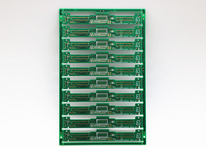
10L HDI 0.1mm Blind Via ENIG 2U'' 2oz Printed Circuit Boards
2. Detailed Specifications
| Material | FR4 |
| Layer | 10L |
| Soldermask | Green |
| Silkscreen | White |
| Finished Board Thickness | 1.6 mm |
| Finished Copper Thickness | 2OZ |
| Surface Treatment | ENIG |
1. Pictures
![]()
![]()
![]()
Contact Person: Mrs. Helen Jiang
Tel: 86-18118756023
Fax: 86-755-85258059