|
|
|
Introduction:
Printed Circuit Board Assembly is to plug the SMT(Surface Mounted Technolofy) and the DIP in the Printed Circuit Board, also called PCBA.
Production:
Both SMT and DIP are means of integrating components in the PCB board. The main difference is that SMT does not need to drill holes on the PCB,while it's nacessary for the DIP to plug the pin of the component into the drilled hole.
SMT:
Mainly use the paste to pack machine to attach some micro components the PCB board. The production process is as follows: the PCB board positioning, solder paste printing, paste and pack, return to the soldering stove, finally inspection.
With the development of science and technology,SMT can also be applied to some large-size components.
DIP:
Insert the componets to the PCB. It is used as a mean to integrate components cause the size is too large to paste and pack, or the manufacturer's production process cannot use SMT technology.
At present, there are two ways to realize manual plug-in and robot plug-in.
The main production processes are as follows: paste back glue (to prevent tin plating to inappropriate places), plug-in, inspection, wave soldering, brush plate (to remove the stain left in the process of passing the furnace) and inspection
printed circuit board manufacturers, pcb assembly shenzhen, pcb factory in China
Product Details:
Payment & Shipping Terms:
|
| Layer Count: | 2 ` 30 Layers | Max Board Size: | 600 Mm X 1200 Mm |
|---|---|---|---|
| Base Material For PCB: | FR4, CEM-1, TACONIC, Aluminium, High Tg Material, High Frequence ROGERS ,TEFLON, ARLON, Halogen-free Material | Rang Of Finish Baords Thickness: | 0.21-7.0mm |
| Minimum Line Width: | 3mil (0.075mm) | Minimum Line Space: | 3mil (0.075mm) |
| Minimum Hole Diameter: | 0.10 Mm | Finishing Treatment: | HASL (Tin-Lead Free), ENIG(Immersion Gold), Immersion Silver , Gold Plating (Flash Gold), OSP, Etc. |
| Thickness Of Copper: | 0.5-14oz (18-490um) | E-Testing: | 100% E-Testing (High Voltage Testing); Flying Probe Testing |
| Layers: | 6Layers | Copper: | 2OZ |
| Material: | FR4 | Surface: | ENIG/HASL |
| High Light: | Automotive BGA PCB Assembly,ODM BGA PCB Assembly,Consumer Electronics PCB Assembly BGA |
||
OEM ODM Service BGA PCB Assembly For Automotive Consumer Electronics
OEM ODM service offer gsm security PCB design/electronic chart design developing
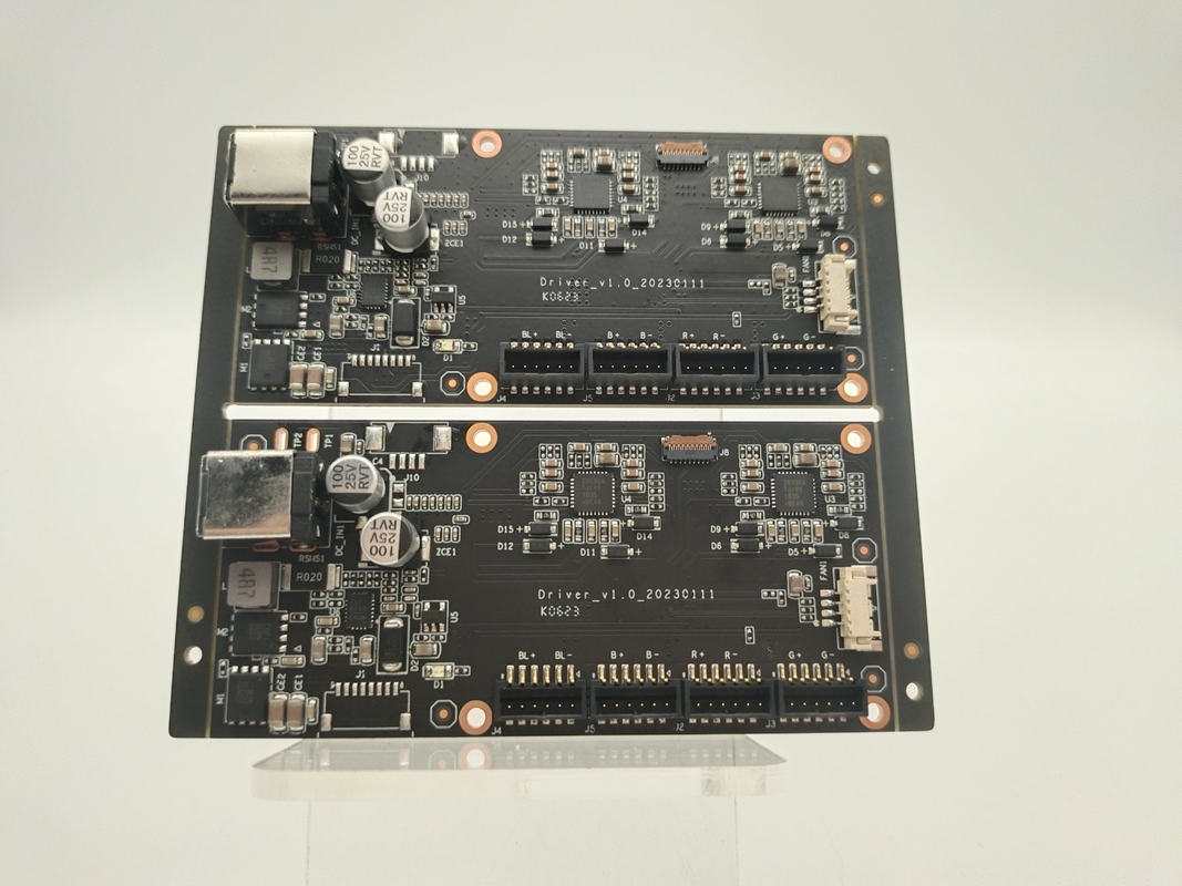
1. Description Of PCB Assembly Service
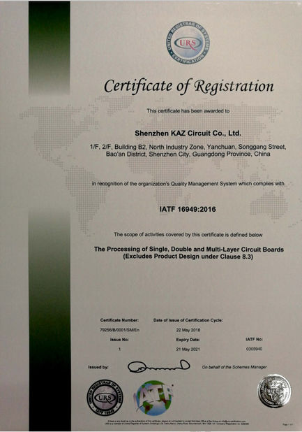
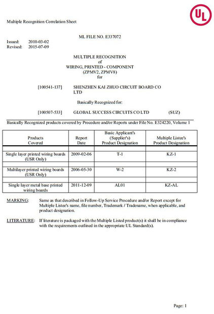
PCB Assembly is 4 layer it is used for security equipment application. we can accept PCB prototype,samll volum, middle and large volume. no MOQ request for new order.all of our PCB are met UL, TS 16949,ROHS, ISO etc. certification.
2. Specification Of PCB Assembly Service
| 1 | Layer | 1-30 layer |
| 2 | Material | FR-4, CEM-1, CEM-3, Hight TG, FR4 Halogen Free, FR-1, FR-2, Aluminum |
| 3 | Board thickness | 0.2mm-7mm |
| 4 | Max.finished board side | 500mm*500mm |
| 5 | Min.drilled hole size | 0.25mm |
| 6 | Min.line width | 0.075mm(3mil) |
| 7 | Min.line spaceing | 0.075mm(3mil) |
| 8 | Surface finish/treatment | HALS/HALS lead free, Chemical tin, Chemical Gold, Immersion gold Inmersion Silver/Gold, Osp, Gold Plating |
| 9 | Copper thickness | 0.5-4.0oz |
| 10 | Solder mask color | green/black/white/red/blue/yellow |
| 11 | Inner packing | Vacuum packing, Plastic bag |
| 12 | Outer packing | Standard carton packing |
| 13 | Hole tolerance | PTH:±0.076, NTPH:±0.05 |
| 14 | Certificate | UL, ISO9001, ISO14001, ROHS, CQC |
| 15 | Profiling Punching | Routing, V-CUT, Beveling |
| 16 | Assembly Service | Providing OEM service to all sorts of printed circuit board assembly |
3. Products Application:
1, Telecom Communication
2, Consumer Electronics
3, Security monitor
4, Vehicle Electronices
5, Smart Home
6, Industrial controls
7, Military & Defense
8, Automotive
9, Smart Home
10, Industrial Automation
11, Medical Devices
12, New Energy
And so on
4. Advantage Of PCB Assembly Service
• Strict product liability, taking IPC-A-160 standard
• Engineering pretreatment before production
• Production process control (5Ms)
• 100% E-test, 100% visual inspection, including IQC, IPQC, FQC, OQC
• 100% AOI inspection, including X-ray, 3D microscope and ICT
• High-voltage test, impedance control test
• Micro section, soldering capacity, thermal stress test, shocking test
5. Picture
![]()
![]()
![]()
6. OEM/ODM/EMS Services For PCBA:
· PCBA, PCB Board assembly: SMT & PTH & BGA
· PCBA and enclosure design
· Components sourcing and purchasing
· Quick prototyping
· Plastic injection molding
· Metal sheet stamping
· Final assembly
· Test: AOI, In-Circuit Test (ICT), Functional Test (FCT)
· Custom clearance for material importing and product exporting
FAQ
Q1: Are you a factory or trading company?
-----We are a factory,Our company is printed circuit board manufacturers.
Q2: Do you accept sample order?
------Yes, we can accept sample order.
Q3: What's your warranty policy?
-----We offer 2 year warranty. For goods defected not by personal seasons, we will replace for it.
Q4: What's your payment terms?
------We accept T/T in advance, paypal, or alipay account.
Q5:What's the lead time for mass order?
------Normally, it takes about 20-35 days, depends on the order quantity.
Contact Person: Mrs. Helen Jiang
Tel: 86-18118756023
Fax: 86-755-85258059