|
|
|
Introduction:
SMT PCB Assembly means Surface Mount Technology, known as a a kind of Circuit assembly technology that installs the SMC/SMD (named Chip Components in Chinese) on the surface of Printed Circuit Board or on the surface of other substrates, which is solded and assembled by means of reflow soldering or dip soldering. It realizes high density, high reliability, miniaturization and low cost of electronic product assembly.
Characterictics:
1. High density, small size, low weight;
2. Reliable, strong earthquake resistance and low defect rate of soldering spot;
3. High frequency, reducting the interference of electromagnetism and radio frequency;
4. Easy to realize automation and improve production efficiency.
Product Details:
Payment & Shipping Terms:
|
| Layers: | 2 Layers | Board Thickness: | 1.6mm |
|---|---|---|---|
| Copper: | 1oz | Surface: | HASL LF |
| Soldmask: | Green | Silk Screen: | White |
prototype development high-mix low-volume production SMT PCB Assembly
Detail Specifications:
| Layers | 2 |
| Material | FR-4 |
| Board Thickness | 1.6mm |
| Copper Thickness | 1oz |
| Surface Treatment | HASL LF |
| Soldmask & Silkscreen | Green & White |
| Quality Standard | IPC Class 2, 100% E-testing |
| Certificates | TS16949, ISO9001, UL, RoHS |
What KAZ Circuit can do for you:
To get a full quotation of the PCB/PCBA, pls provide the information as below:
Manufacturer Capacity:
| Capacity | Double Sided: 12000 sq.m / month Multilayers: 8000sq.m / month |
| Min Line Width/Gap | 4/4 mil (1mil=0.0254mm) |
| Board Thickness | 0.3~4.0mm |
| Layers | 1~20 layers |
| Material | FR-4, Aluminum, PI |
| Copper Thickness | 0.5~4oz |
| Material Tg | Tg140~Tg170 |
| Max PCB Size | 600*1200mm |
| Min Hole Size | 0.2mm (+/- 0.025) |
| Surface Treatment | HASL, ENIG, OSP |
SMT Capacity
![]()
Prototype development high-mix low-volume production SMT PCB Assembly
Definition:
Prototype development high-mix low-volume production SMT PCB assembly refers to the process of assembling printed circuit boards (PCBs) for prototype development and low-volume production runs using surface mount technology (SMT). SMT is a method of assembling electronic components directly onto the surface of a PCB, rather than inserting them into holes in the board.
Applications:
Prototype development high-mix low-volume production SMT PCB assembly is ideal for:
Creating prototypes of new electronic products
Producing small batches of custom PCBs
Manufacturing low-volume production runs of PCBs
Advantages:
Reduced size and weight: SMT components are smaller and lighter than traditional through-hole components, resulting in smaller and lighter PCBs.
Higher density: SMT allows for a higher density of components on a PCB, enabling more functionality in a smaller space.
Improved performance: SMT components have shorter leads, which reduces inductance and capacitance, leading to improved signal integrity and performance.
Lower cost: SMT assembly is more automated than traditional through-hole assembly, resulting in lower labor costs.
Increased reliability: SMT components are less likely to experience solder joint failures due to the shorter leads and more precise soldering process.
Process:
The prototype development high-mix low-volume production SMT PCB assembly process typically involves the following steps:
Design: The PCB is designed using computer-aided design (CAD) software.
Fabrication: The PCB is fabricated using a process called photolithography.
Solder paste application: Solder paste is applied to the PCB at the locations where the components will be placed.
Component placement: SMT components are placed on the PCB using a pick-and-place machine.
Reflow soldering: The PCB is passed through a reflow oven, which heats the solder paste and reflows it, forming solder joints between the components and the PCB.
Inspection: The PCB
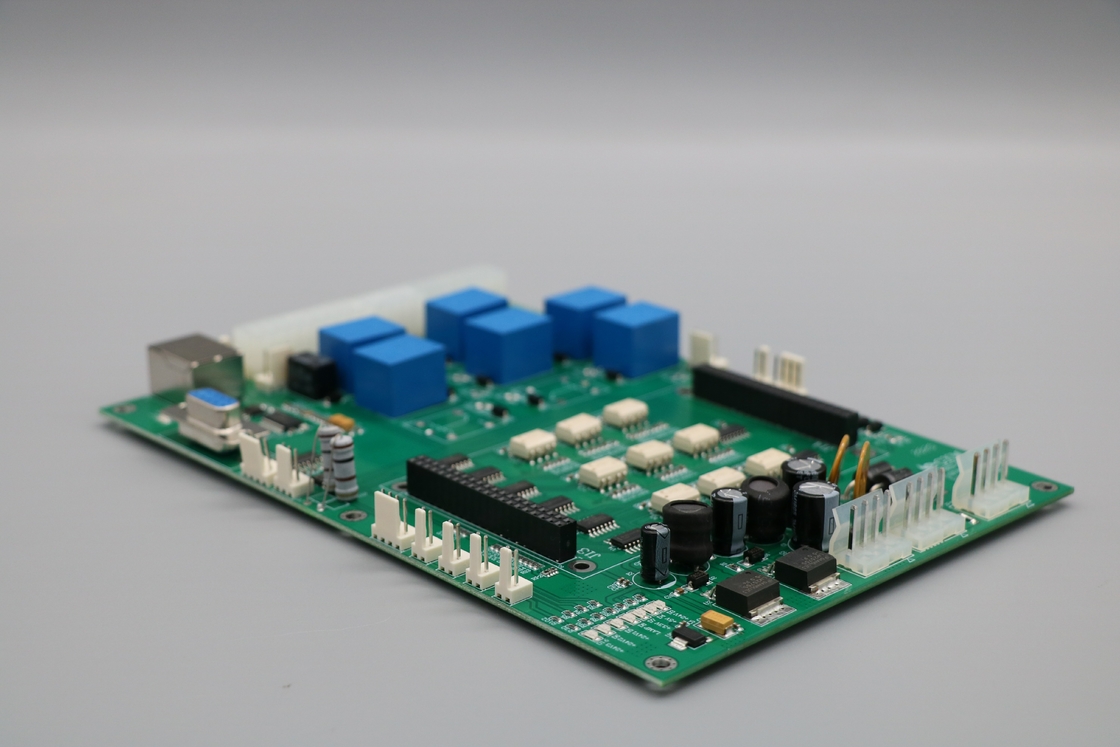
Photoes of this prototype development high-mix low-volume production SMT PCB Assembly
![]()
![]()
![]()
![]()
Contact Person: Stacey Zhao
Tel: +86 13392447006
Fax: 86-755-85258059