|
|
|
HDI PCB is the shortened form of High Density Interconnector PCB. It's a technology of printed circuit board production.
It uses the micro blind & buried vias technology with high density circuits layout on the PCB board. It's a compact PCB that is designed for small volume users. It uses the design of modular paralle capacity of 1000VA, say height of 1u, natural cooling down, and it can be placed into the rack of 19" directly, the max parallel that can be connected in is up to 6 modules. This special products uses all digital signal processing (DSP) technology and multiple patented technology, it has the ful range of adaptability to load capacity and strong short-term overload capacity, and can ignore the factor of load power and crest.
Advantages of HDI PCB can be small size, high frequency and high speed. Mainly used for PC, cellphones and digital cameras...
Product Details:
Payment & Shipping Terms:
|
| Material: | FR-4 | Layers: | 10 Layers |
|---|---|---|---|
| Board Thickness: | 1.6mm | Copper: | 1oz |
| Surface: | ENIG | Soldmask: | Black |
| Silk Screen: | White | Standard Testing: | IPC Class 2 |
| High Light: | blind via pcb,lead free pcb |
||
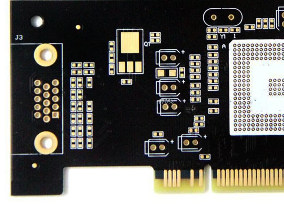
FR4 Electronic Circuit Board HDI Golden Finger PCB
Detail Specifications:
| Layers | 10 |
| Material | FR-4 |
| Board Thickness | 1.6mm |
| Copper Thickness | 1oz |
| Surface Treatment | HASL LF |
| Soldmask & Silkscreen | Green & White |
| Quality Standard | IPC Class 2, 100% E-testing |
| Certificates | TS16949, ISO9001, UL, RoHS |
What KAZ Circuit can do for you:
To get a full quotation of the PCB/PCBA, pls provide the information as below:
Company Informaiton:
KAZ Circuit is a professional PCB manufacturer from China since 2007, also provide PCB Assembly service for our customers. Now with about 300 employees. Certified with ISO9001,TS16949, UL, RoHS. We are confident to provide you quality products with factory-directed price within the fastest delivery time!
Manufacturer Capacity:
| Capacity | Double Sided: 12000 sq.m / month Multilayers: 8000sq.m / month |
| Min Line Width/Gap | 4/4 mil (1mil=0.0254mm) |
| Board Thickness | 0.3~4.0mm |
| Layers | 1~20 layers |
| Material | FR-4, Aluminum, PI |
| Copper Thickness | 0.5~4oz |
| Material Tg | Tg140~Tg170 |
| Max PCB Size | 600*1200mm |
| Min Hole Size | 0.2mm (+/- 0.025) |
| Surface Treatment | HASL, ENIG, OSP |
SMT Capacity
![]()
More Photo of this High quality FR4 electronic circuit board HDI PCB with golden finger
![]()
Contact Person: Jesson
Tel: 8613570891588
Fax: 86-755-85258059