|
|
|
Introduction:
Power Supply PCB means that the PCB is applied to the power supply produc, such as power bank, switching power supply and so on. It is usually with heavy copper thickness (2oz, 3oz or heavier).
Working Layer:
The circuit board includes many types of working layers, such as the signal layer, protection layer, Silkscreen layer and inner layer, etc. The functions of various layers are briefly introduced as follows:
1. Signal layer: mainly used to place components or wiring.
2. Protection layer: mainly used to ensure that the circuit board does not need to be tin-coated, to ensure the reliability of the circuit board operation.
3. Silkscreen layer: mainly used in the printed circuit board components on the serial number, production number and company name.
4. Inner layer: mainly used as signal wiring layer
5. Other layers: mainly includes four types of layers as following:
Drill Guide (Drill orifice layer) : used primarily for Drill positions on printed circuit boards.
Keep-out Layer: mainly used to draw the electrical frame of the circuit board.
Product Details:
Payment & Shipping Terms:
|
| Application: | EMS | Material: | FR4 KB |
|---|---|---|---|
| Production Name: | Printede Circuit Board | SMT: | Support |
| Type: | Multilayer | The Min Hole: | 0.15mm |
| High Light: | printed circuit board pcb,power supply circuit board |
||
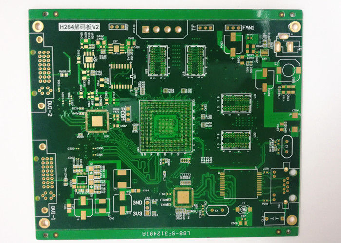
Multilayer Heavy Copper 2OZ~8OZ ENIG 2U' Rigid FR4 PCB board
1.Features
1. One Stop OEM Service: Made in Shenzhen of China
2. Manufactured by Gerber File and Bom LIst Offered by Customers
3. SMT, DIP Technology Support
4. FR4 Material Meet 94v0 Standard
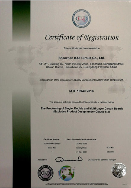
5. UL,CE,ROHS Compliant
6. Standard Lead Time: 4-5days for 2L;5-7 for 4L. Expedited Service is available
2.Detailed Specification
| Material | FR4 KB |
| Finished Copper Thickness | 1oz |
| Finished Board Thickness | 0.8-1.6mm |
| The Min Hole | 0.15mm |
| Silkscreen | White |
| Solder Mask | Green |
| Surface Treatment | ENIG 2U' |
| Layer | 6 L |
A "Multilayer Heavy Copper 2OZ~8OZ ENIG 2U' Rigid FR4 PCB Board" refers to a specific type of printed circuit board (PCB) with several characteristics. Let's break down each component:
Multilayer: This indicates that the PCB has multiple layers of conductive material separated by insulating layers. Multilayer PCBs allow for complex circuit designs with improved signal integrity, reduced size, and increased functionality.
Heavy Copper: "Heavy Copper" refers to the copper weight or thickness of the copper traces on the PCB. The term "heavy copper" is used when the copper weight is higher than the standard weight used in regular PCBs. Heavy copper PCBs are designed to carry higher currents and withstand higher temperatures. The copper weight can range from 2 ounces (2OZ) to 8 ounces (8OZ) or even higher.
ENIG: ENIG stands for Electroless Nickel Immersion Gold, which is a type of surface finish used on PCBs. The ENIG process involves depositing a thin layer of nickel onto the exposed copper surfaces, followed by a layer of gold. ENIG provides excellent solderability, corrosion resistance, and flatness of the surface.
2U': "2U'" refers to the thickness of the gold layer in the ENIG surface finish and is expressed in micrometers (µm). A 2U' thickness is relatively standard and offers good protection and solderability for the PCB.
Rigid FR4: "Rigid" indicates that the PCB is not flexible, providing a solid and sturdy structure. FR4 is a commonly used PCB substrate material made of a glass-reinforced epoxy laminate. It offers good electrical insulation properties, mechanical strength, and flame resistance.
In summary, a "Multilayer Heavy Copper 2OZ~8OZ ENIG 2U' Rigid FR4 PCB Board" refers to a rigid PCB with multiple layers, heavy copper traces ranging from 2 to 8 ounces, an ENIG surface finish with a 2µm gold thickness, and an FR4 substrate material. This type of PCB is suitable for applications that require high current-carrying capacity, thermal management, and durability. It is commonly used in power electronics, automotive applications, industrial equipment, and other demanding environments.
3. Pictures for Multilayer Heavy Copper 2OZ~8OZ ENIG 2U' Rigid FR4 PCB board
![]()
![]()
![]()
![]()
Contact Person: Stacey Zhao
Tel: +86 13392447006
Fax: 86-755-85258059